Overview
Since 1995, 30 years at the forefront of tooling innovation.
We are an international, ISO 9001:2015 certified precision engineering company founded in 1995 by Mr. HP Tan. We supply high-precision tooling to the semiconductor, connector, and stamping sectors of the electronics industry. In 2023, TOWA Corporation, a leading Japanese OEM in semiconductor auto-molding and packaging equipment, acquired our semiconductor mold division: a customer validation of the precision multinational manufacturers expect from us.
Mission and vision
What drives us
Delivering precision engineering solutions with uncompromising quality and speed, transforming our clients' complex designs into perfectly manufactured components with advanced technology and decades of expertise.
Where we're headed
We envision a future where we are the precision engineering partner that innovators from all over the world trust first, known for solving difficult challenges through technical excellence and genuine, transparent partnership.
Values
We operate every project with these firm principles in mind.
Our commitment to our core values helps us to deliver exceptional results every time - values that we live by during every project we take on and every relationship we build.
History
We have made significant improvements since our founding.
We have continuously improved our processes, embraced new technologies, and expanded our workspaces to better serve our clients and adapt to the ever-changing market demands.
Establishment (1995)
We began as a small, humble workshop in a rented space, initially focused on producing spare parts. Since then, we've experienced rapid growth in both our workforce and machinery.


First factory (1997)
Just two years later, we moved into our own 12,000 square foot semi-detached factory in Bayan Lepas, a thriving industrial hub on the island of Penang in Malaysia. This allowed us to expand our production capabilities and better serve our growing client base.
Bigger factory (2010)
After seeing continued success from our first factory, we expanded into an advanced 28,000 square foot facility, also in Bayan Lepas, to support our continued growth and innovation.

Sale of division (2023)
We sold our semiconductor mold division to TOWA Corporation, a leading Japanese OEM in semiconductor auto-molding and packaging equipment. This enabled us to concentrate on ultra-precision engineering in the stamping and connector industry.

An even bigger facility (2025)
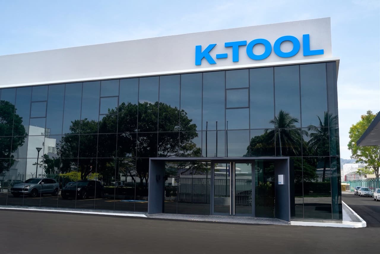
We commissioned a 50,000 square foot state-of-the-art facility to further elevate our capabilities and strengthen our position as a leader in ultra-precision manufacturing in Malaysia.

Why Penang
Manufacturing from Penang, Malaysia's semiconductor manufacturing hub gives our customers a logistical edge.
A supplier decision is also a location decision. Manufacturing out of Penang gives our semiconductor, connector, and test customers four concrete advantages.
Proximity to your Asian operations
Penang sits within a few hours' flight of major semiconductor and electronics manufacturing hubs across Asia, shortening the loop between your design teams and our shop floor.
Free trade zone logistics
Bayan Lepas Industrial Park is a licensed Free Industrial Zone, streamlining duty-free import of raw materials and export of finished tooling to your facilities.
An established precision engineering talent pool
Penang's electronics industry has trained toolmakers, machinists, and metrology technicians for over four decades, the workforce our processes depend on.
Decades of MNC supplier culture
We operate under the same quality, documentation, and audit expectations multinational semiconductor and connector manufacturers have required of Penang-based suppliers since the 1970s.
Contact
How can we help?
If you have general inquiries about us and what we do, please fill in the form on the right and we'll get in touch with you as soon as we can.
However, if you already have a project or specific requirements in mind, please let us know here.