Precision engineering
Precision Engineering for Semiconductor: Test, Burn-In and Packaging Tooling Machined in Penang
Test, burn-in and packaging tooling machined in Penang: what it involves and how to choose a shop.
Malaysia handles around 13% of the world's semiconductor assembly, testing and packaging volume, and most of it moves through plants within an hour of Bayan Lepas. Every one of those plants runs on precision tooling: test sockets, burn-in hardware, mold chases, singulation tooling, handler change kits. When that tooling wears, breaks or needs an engineering change, the line waits.
This post explains what precision engineering for semiconductor tooling actually involves, which components the back-end consumes, and what to check when sourcing a machining partner for them.
What does precision engineering mean in semiconductor back-end?
In this context, precision engineering means machining components in materials such as hardened tool steel, tungsten carbide, stainless steel and engineering plastics to tolerances between ±0.001mm and ±0.005mm, with the surface finish, flatness and edge condition that test and packaging hardware demands.
The processes behind it are the classic toolroom set, applied at semiconductor tolerances: CNC milling for blanks and prismatic features, wire EDM for hardened profiles and apertures, sinker EDM for cavities and blind features, and grinding, surface and profile, for the flatness, parallelism and final form accuracy that decides whether the assembly works. Parts are machined soft, hardened, then finished by EDM and grinding after heat treatment so distortion is ground out rather than shipped out.
That toolroom work feeds every step a chip passes through between the wafer fab and the circuit board, and each step depends on precision tooling.
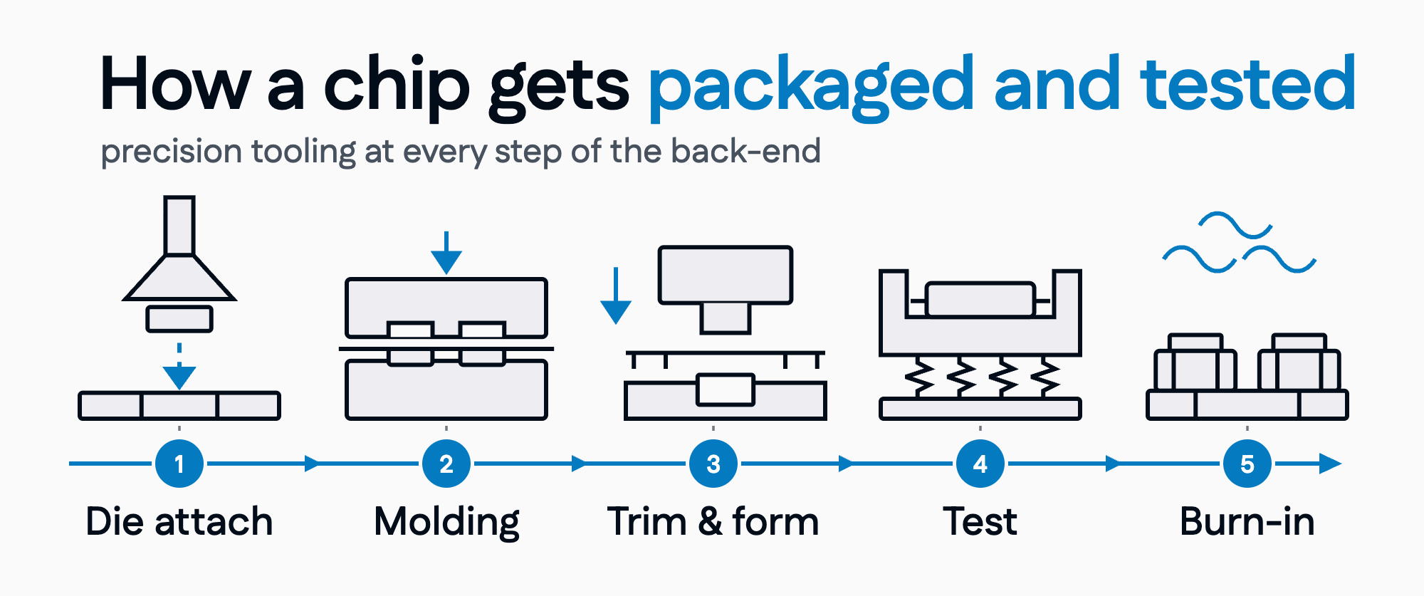
The sections below start at the end of that line, with test and burn-in, then work back to assembly and packaging.
Tooling for semiconductor test and burn-in
Test is the most tooling-hungry stage of the back-end, because everything that touches the device under test is a wear part.
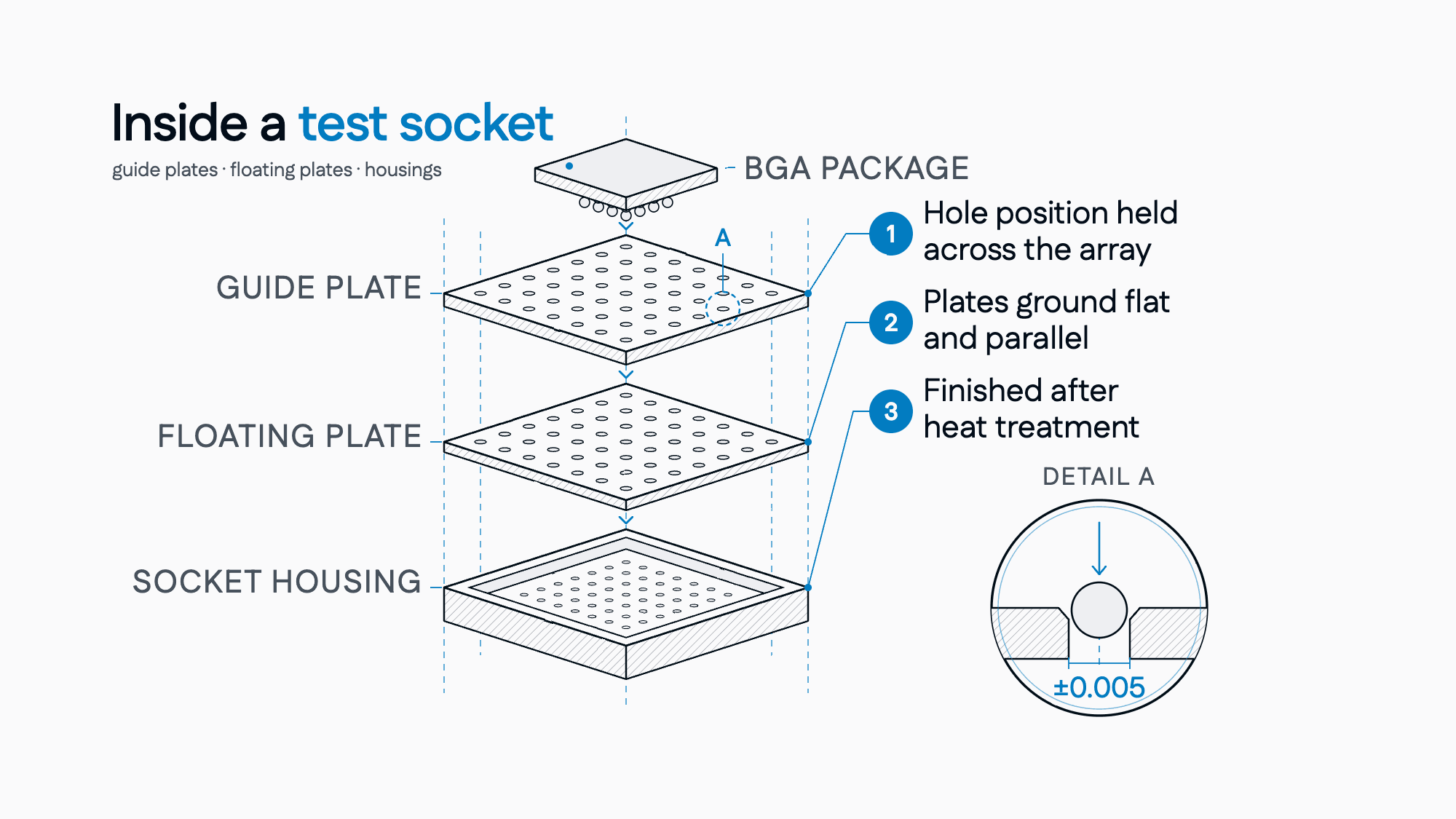
Test sockets and contactors, like the one pictured at the top of this post, carry guide plates, floating plates and housings machined in hardened steel, stainless and engineering plastics. Hole position across the array must match the package ball or lead map, and plates must sit flat and parallel so contact force is even across every pin.
Burn-in tooling runs the same geometry at elevated temperature for hours, which pushes material choice toward grades that hold dimension when hot and pushes tolerances onto the machining rather than adjustment at assembly.
Handler and prober change kits, nests, pushers, seating plates and alignment components, are what convert a generic machine to a specific package. New package ramps mean new kits, usually wanted quickly and in small quantities.
Typical parts:
- Socket guide plates, floating plates and housings
- Burn-in board hardware and high-temperature socket components
- Handler change kits, nests and alignment tooling
Tooling for assembly and packaging
Packaging tooling is where mold making and stamping die work meet the semiconductor line.
Encapsulation mold chases and inserts form the package body. Cavity dimensions, shut-off surfaces and venting all sit in hardened steel, machined by sinker EDM and finished by grinding, where a shut-off ground to the right flatness is the difference between a clean package and flash on every shot.
Trim and form tooling, punches and die inserts that cut and shape leads after molding, is carbide and tool steel stamping work. Lead frame tooling holds punch-to-die clearances of a few microns per side on thin material, which is why these punches are wire EDM roughed and profile ground to ±0.001mm, a process split we cover in detail in profile grinding vs wire EDM.
Singulation and die-attach hardware, from saw jigs and chucks to epoxy stamping and pick-up tooling, rounds out the set: small, accurate, hardened components consumed steadily by every assembly line.
Typical parts:
- Trim and form punches and die inserts for lead frames
- Singulation jigs, chucks and die-attach tooling
Why source semiconductor tooling in Malaysia?
The practical case is proximity to the work. With Malaysia carrying roughly 13% of global assembly, testing and packaging volume, per the Malaysian Investment Development Authority, the plants consuming this tooling are concentrated in Penang, Kulim, Melaka and Johor. A tooling partner inside that ecosystem is hours from the line, not a customs cycle away. That matters most on urgent jobs: a cracked punch on a qualified trim and form tool, or a change kit for a ramp that moved forward a month.
The supporting trades grew up alongside the plants. Heat treatment, coating, carbide blank supply and calibration services all exist locally with short lead times, so the full process chain runs domestically. For overseas tooling groups, the region offers competitive costs, English-language engineering communication and a long history of supplying multinational manufacturers.
There is also accumulated product knowledge. Penang has supported semiconductor back-end plants for decades, so local toolmakers are used to reading test and packaging tooling drawings, spotting datum or clearance issues before cutting, and knowing which tolerances matter to the function.
How to choose a machining partner for semiconductor tooling
Most machining shops list similar certificates and machines, so it helps to ask a few specific questions when comparing suppliers.
Do they finish after heat treatment? Test and packaging tooling is usually hardened, and hardening moves the part. Critical features should be finished by wire EDM, sinker EDM or grinding after heat treatment, with grinding stock allowed for from the start.
Can they hold position across the whole array? A hole diameter tolerance is only part of the picture. Socket and guide plate work depends on positional accuracy across hundreds of features, which comes down to machine stability and datum strategy. Ask how position is controlled and verified across a full plate.
What do they measure with? Tolerances of ±0.001mm to ±0.005mm are only meaningful if the measuring equipment can resolve them and calibration is traceable. Ask what equipment inspects the work and what report comes with it.
How much of the process is done in-house? When milling, EDM, grinding and inspection happen in one shop, one datum strategy runs through the job and one party is responsible for the tolerance stack. When steps are subcontracted, ask how datums and tolerances are managed between suppliers.
Have they been through customer audits? Semiconductor manufacturers audit their suppliers closely, so experience with those audits is a useful sign that a shop's quality system works in practice, not just on paper.
Semiconductor tooling at K-TOOL
K-TOOL Engineering is an ISO 9001:2015 certified precision machining shop in Bayan Lepas Industrial Park, Penang, and has been machining tooling for over thirty years. Our work for test, burn-in and packaging covers socket and guide plates and trim-and-form punches and dies, using CNC milling, wire EDM, sinker EDM and profile grinding in-house. Ground profiles in carbide and tool steel are held to ±0.001mm, and parts are finished after heat treatment and inspected on calibrated equipment.
Our quality system is covered on the quality assurance page, and the wider capability picture in our precision engineering in Malaysia overview. If you have a tooling drawing you would like us to look at, you can send it through our quote page.
Frequently asked questions
What tolerances does semiconductor test tooling need?
Typical machining tolerances run from ±0.001mm to ±0.005mm depending on the component. Ground punch profiles and precision inserts sit at the tight end, at ±0.001mm, while housings and structural components sit looser. The drawing governs; specifying tighter than the function needs only adds cost.
What materials are used for test sockets and packaging tooling?
Hardened tool steels such as SKD11, D2 and H13, stainless grades, and tungsten carbide for high-wear features like trim punches and die inserts. Burn-in hardware favours grades that hold dimension at temperature. Engineering plastics appear in socket components, machined alongside the metalwork.
Can you make replacement tooling from a worn part or an old drawing?
Usually, yes. With the original drawing the job is straightforward. With only a worn sample, the part can be measured and re-drawn, with wear-critical features restored to nominal rather than copied worn. If you have either, we can confirm what is needed.
How fast can replacement tooling be delivered in Malaysia?
It depends on material, hardening and scope, but being in Bayan Lepas means urgent single-piece replacements for local plants can often be turned around in days rather than weeks. Lead time is confirmed once we have seen the drawing.